LAB 02
Solderless Breadboard
555 Timer Lab Report — NE555 vs TLC555
This lab compares the NE555 bipolar timer and the TLC555 CMOS timer in astable mode.
I built the circuit on a solderless breadboard, measured frequency, rise time, fall time,
and LED load current, and then selected the better timer for the PCB design.
≈463 Hz
NE555 measured frequency
89 ns
NE555 rise time
14.8 ns
TLC555 rise time
NE555
selected for PCB design
Step 01
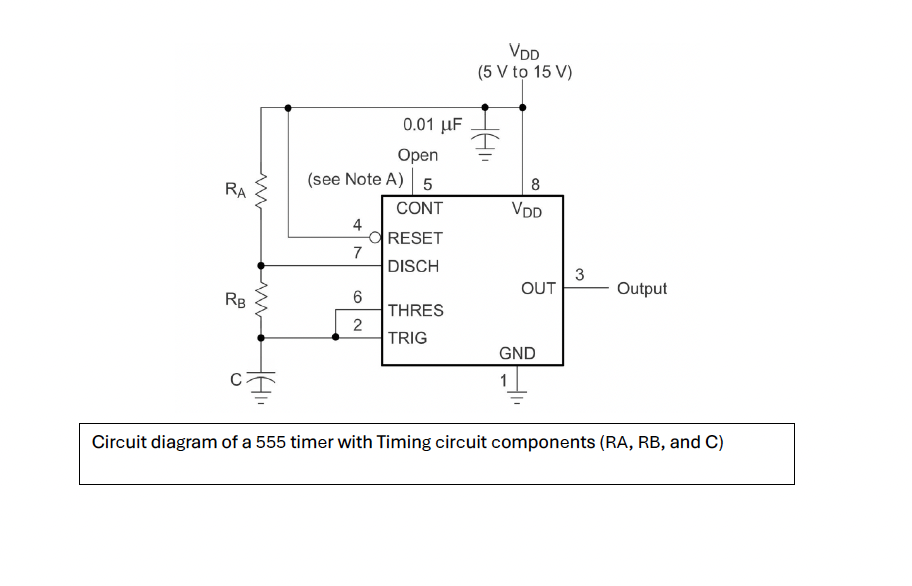
Understand the 555 Timer Circuit
A 555 timer can generate a repeating square wave without an external trigger. The frequency and duty cycle are controlled by two resistors, RA and RB, and one timing capacitor. This makes the 555 timer useful for blinking LEDs, clock pulses, tone generation, and PWM-style timing.
Step 02
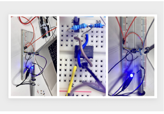
Build the Circuit on a Solderless Breadboard
I placed the 555 timer circuit on a solderless breadboard and powered it with 5 VDC. The output was connected to the oscilloscope so I could measure frequency, duty cycle, rise time, fall time, and LED load current using different resistors.
Step 03
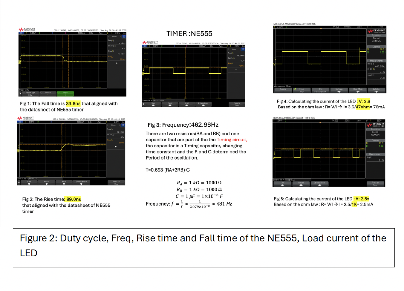
Measure the NE555 Timer
For the NE555 timer, the measured frequency was about 463 Hz, close to the theoretical value of about 481 Hz for RA = 1 kΩ, RB = 1 kΩ, and C = 1 µF. The measured rise time was 89 ns, and the fall time was 33.8 ns. The NE555 also provided higher output current when driving the LED load.
Step 04
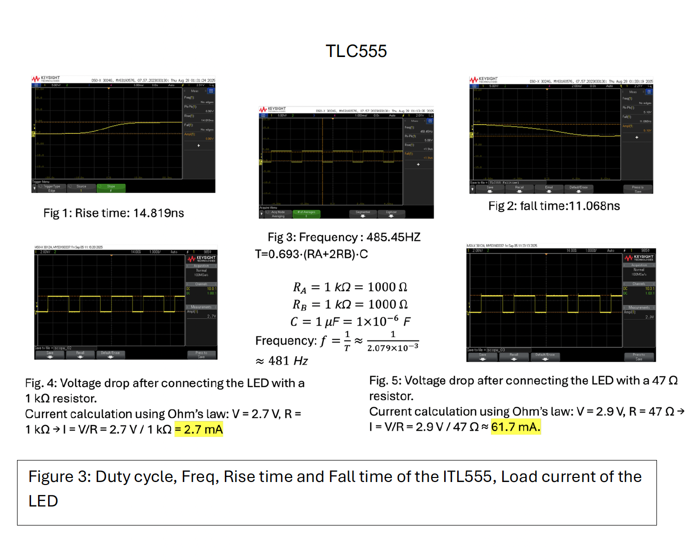
Measure the TLC555 Timer
I repeated the same test with the TLC555 CMOS timer. The measured frequency was close to the NE555 result, but the TLC555 switched much faster. The measured rise time was about 14.8 ns, and the fall time was about 11.1 ns.
Step 05
Compare the Results
Both timers produced nearly the same oscillation frequency, but their output behavior was different. The TLC555 had faster switching edges, while the NE555 provided stronger current drive for the LED load.
| Measurement | NE555 | TLC555 |
|---|
| Rise time | 89 ns | 14.8 ns |
| Fall time | 33.8 ns | 11.1 ns |
| Frequency | ≈463 Hz | ≈485 Hz |
| LED current with 1 kΩ | 2.5 mA | 2.7 mA |
| LED current with 47 Ω | 76 mA | 61.7 mA |
Step 06
Final Decision for PCB Design
Why I selected the NE555
- The TLC555 is faster and produces sharper switching edges.
- The NE555 provides stronger current drive, which is useful for driving LED loads.
- The NE555 rise and fall times are still acceptable because the target frequency is only around 500 Hz.
- For the PCB design, the NE555 was selected because it is more robust for this load-driving application.
NE555TLC555Astable Mode
OscilloscopeBreadboardPCB Decision